Design and text by:- Mike Brown
Date: 1st June 1996, Version 1.02
Thanks also to Fabrice Frances and Jon Haworth for helping with some of the "detail niggling" to get to V1.02. Also, since V1.01 I've been confirming some of the timings etc. using an oscilloscope on a real Oric, and so these are now more accurate. This is reflected in a few design changes, and also a few additions.
Technical note:- A ULA or "Gate Array" is formed from a chip made entirely of (for example) thousands of NAND gates, all laid out, but unconnected. Each specific application requires a set of metal track deposited to complete the circuit, done at manufacturer as a final step.
The ULA performs several "visible" tasks which are closely integrated. These are:-
o Address Decode Logic Select lines for VIA chip, ROM, RAM areas of memory subject to state of ~MAP signal.
o Bus Clock signal production Division of 12MHz source clock into 1 MHz processor clock, internal 6 MHz dot clock
o Memory Multiplex (6502 versus Video arbitration) Interleaving of access to DRAM on two halves of 6502 cycle, one half to a single 6502 access, the other to one (or, in lores/text two) video accesses. Further multiplex of 16 bit addresses to 8 bit Row and Column format for DRAM
o Video signal production Acquiring video data from DRAM, conversion to pixel data via character sets (for lores modes), output as RGB ink and paper values Provision of sync signals for display device
o Memory Refresh Side effect of rapid sequential access to DRAM by video circuitry, causes every row to be guaranteed to be read within the required time.
o Control/Sequencing Externally, provides ~RAS ~CAS and R/~W control signals for DRAM along with row and column addresses from multiplexer. Internally sequences movement of data through ULA
Operation:
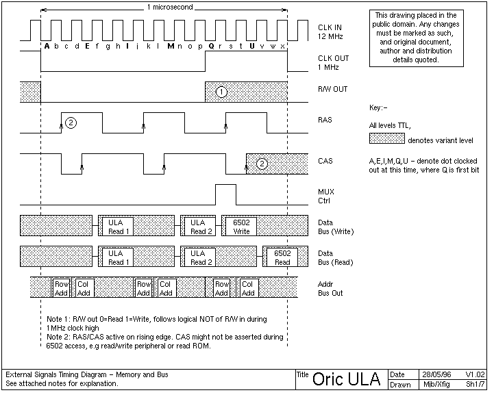
The crystal generated 12MHz clock in Oric is fed to the ULA at pin 7. This is used by the control logic later, and divided by 2 to provide the dot clock used for building of the TV picture. This is then further divided by 6 to provide the 1 MHz clock for the system, found at pin 14. Note that in the timing diagrams of sheet 1, the 1 MHz clock is assymetric, and this is why a 2MHz part is used in Oric. The effective time available to the 6502 is that of a 1.5MHz clock, with the ULA taking more than half the cycle.
To generate the picture, we require two counters to count our position across and down the screen. The first of these is a 6 bit counter, and this is clocked at 1 MHz, counting a total of 64us across one complete scan line of the picture. Although it may be conceptually easier to view each scanline starting at 0 end ending at 63, it is simpler for design purposes to start the video waveform at count=0 and displace blanking and sync to the end of the count. Also note that the position and width of the sync pulse (horizontal and vertical) is placed approximately half way along the blank portion.
Each column of Oric's screen is represented by 1us of time, subdivided into groups of 6 pixels. From this 6 bit counter, combinatorial logic is used to derive sync and blanking signals. The blanking signal is used both to suppress video outside of the screen area (border, flyback etc.). The sync signal is provided to synchronise the display device to the internal counters.
The remaining signal, SelReload, resets 3 of the registers to default values at the start of each scanline. These are r0, ink = 111b, r1, style=000b and r2, paper=000b).
The second counter increments for each complete line scanned, and counts through one of two numbers of cycles, depending on the refresh rate in force (50/60Hz). This too uses combinatorial logic to derive sync/blank signals, and further an end of vertical frame signal, which resets the counter after either 312 (50 Hz) or 260 (60 Hz) lines. For HIRES mode, a signal which identifies line 200 (the beginning of the text area) is derived. This is used to set a latch forcing certain behaviour for the end of screen, see later.
Each time the vertical counter is reset, a further counter/divider is clocked, counting 32 frames before toggling. This is later used to implement flashing graphics.
The individual sync and blanking signals are combined to provide a composite sync video signal at pin 16, and an internal composite blanking signal.
For Combinatorial Block A, the logic can be described from the timing information gathered as:-
HBLANK = H5 AND ( H4 OR H3 )
HSYNC = H5 AND H4 AND ~H3 AND ( ( ~H1 AND ~H0 ) XOR H2 )
SELREL = H5 AND H4 AND H3
For Block B:- (50 Hz operation)
VBLANK = V5 AND V6 AND V7
VSYNC = V8 AND V2
VFRAME = V8 AND V3 AND V4 AND V5
where Hx and Vx are bit x of the Horizontal or Vertical Count
The vertical count is then processed according to graphics mode and whether double height text is selected.
Ignoring the "divide by 2 block" for the moment, normal text processing proceeds as follows. The address to be fetched from the screen is calculated from the text line down the screen (b3-b7) multiplied by 40, plus the text column across (b0-5 of horiz counter). Two points - the divide by 8 of vertical count is to cast aside the 3 bits expressing which scan line we are on - this has no bearing on the lookup address for the ASCII code, but does on the character definition later, hence these 3 bits are preserved as "Character Row Count". Multiply by 40 is expressed as a multiply by 10, and then a bit shift of 2 (hardware implemented by skew-wiring).
In text mode, when double height text is selected, this is effected by causing the character lookup to lookup the same scan line twice in the character definitions (this draws the one half of the letter filling one line). Although the vertical count is being "altered", the screen will still continue to scan out as normal, and so lines end up duplicated during the double height period. The lowest bit of the "row number" (found in b3-b7) is shifted over into b2 in this process, causing even lines to have the top half of the character (scan lines 0-3) and the odd lines to have the bottom half (lines 4-7). This gives an assumption that all text starts on even lines, and explains the bug where bottom halves of text appear above the top half.
When the 13 bit result is calculated, the base of the screen address is then added (a constant BB80hex for text/lores) and the address is ready as "Video Address Phase 1". The process so far acquires the ASCII character only, and is the precursor to "Character Definition Lookup".
In hires mode, the address to be fetched is calculated from the scan line down (we include the three bits removed for text mode), also multiplied by 40. The base address for the hires screen is added (constant A000hex) and the address is ready as "Video Address Phase 1".
Observations and Notes: As we know that the counters and addition circuits will be limited to certain values, the number of bits can be limited. I have checked thoroughly that there are enough bits to successfully work, even though it may appear that some sections are one bit short. F.E. - 9 bit vertical counter needs to be able to keep time for about 260 or 312 lines, however our usable picture area, top to bottom, is only 0-223 lines, so only 8 bits need processing by the memory mapper. All 9 bits are available to the combinatory logic.
Division by 2 and 8 blocks - I picture these like "switches" that either route straight through, or 1 (3) bits right. At chip level these would be routing transistors.
Although no fetch [should] happen, as the counter reaches column 40->63 the memory mapper will continue to lookup data. This in fact models the real ULA correctly, from experiment. Also, the ULA continues to lookup character definitions when an attribute is found, and during hires mode, although this information is not actually used.
While developing this, I also noticed that if the HIRES screen didn't have some lines of text at the bottom, it would actually run off the end of its allotted area (A000 hex to BFE0 hex). e.g. Line 200 is at #BF40, 201 = #BF68, 202 = #BF90, 203 = #BFB8, 204 is into "unknown" territory, and is therefore suspect, 205 is into the ROM! (#C008). But, the total number of theoretically available lines is 200 + (8*3) = 224. So are the text lines a necessary thing? What if you program a screen which is entirely HIRES? Or has only one text line? Do you see junk between line 204 and the start of your text line?
The answer to this came in the form of a small redesign around the text/hires selection. The real ULA forces hires to end at line 200 irrespective of attributes prevailing at the time. The text/hires selector output is therefore modified to text for lines 200 onward, hence you can have more than 3 lines, but not less. Note that this affects four things :-
o In HIRES mode, hires part of screen, double height is ignored
text part of screen, double height operates
In TEXT mode double height always operates
o In HIRES mode, hires part of screen, vertical count is used directly
text part of screen, vertical count is divided by 8 as per:-
TEXT mode where vertical count divides by 8, described above.
o In HIRES mode, hires part of screen, the base address of calcs is A000hex
text part of screen, the base address is BB80h
TEXT mode Base address is BB80h
o In HIRES mode, hires part of screen, control and seq looks up char defs,
and then does not use them.
text part of screen, these are used as bit data
o In TEXT mode these are used as bit data
The line-200 force does *not* affect the base address of the character set.
o In HIRES mode, hires*or*text part, lower address (9800h) used
In TEXT mode, upper address (B400h) used.
Operation:
The address decode block provides two signals for external enables. A8 through A15 (pins 32,33,31,15,35,22,29,30), 1 MHz clock and MAP (pin 26) are used to derive enable signals for the ROM and VIA chip :-
When the address present on the bus is in the range 0300h-03FFh, I/O (pin 25) is taken low.
When the address present is in the range C000h-FFFFh, ROM select (pin 23) is taken low, unless MAP is asserted. In this case, the address will be treated as a normal RAM address allowing access to the "shadow" ram at C000h-FFFFh.
When the address is in the range 0000h-BFFFh, it is taken as a normal ram access, unless MAP is asserted. In this case, no RAM access takes place (this is to allow external peripherals to drive the data bus for data reads)
The external data bus, D0-D7 (pins 8,17,11,12,13,5,34,18) is buffered into the chip onto an internal databus. Note that the ULA never outputs data to the bus.
When in HIRES mode, the video address generated in phase 1 is outputted (see memory mux/control for description) and the data fetched is interpreted either as an attribute (see later), or literal pixel layout. This is loaded to a holding register for later loading to the shift register for output. For an attribute, 0 is loaded to the holding register (all paper colour). bit 7 is available to the video inverter on loading of the shift register, and if set, inverts the video. For an attribute, Load 0 is used to ensure no video inversion takes place.
For text mode, a further stage must be done. The video address (phase 1) points to an ASCII value, which is fetched, multiplied by 8, has the "Character Row" count (0-7) added to it. This gives an offset into the character definition. A base address is added (9800h hires mode, B400h text mode) and an offset for standard or alternate character set (0h or 400h) before a 16bit Video Address Phase 2 is generated. This is output as for the phase 1 address, and the resulting data is now a bit pattern to go to the holding/shift registers.
The fetched data, if an attribute, is used to update one of four registers inside the ULA. These 3 bit registers hold the ink and paper colours, the "style", and the "mode". The allocation is :-
Reg Name b0=1(0) b1=1(0) b2=1(0)
r0 Ink Colour R G B
r1 Style Alt(Std) Dbl(Std) Flash(Std)
r2 Paper Colour R G B
r3 Mode xxx 50Hz(60Hz) Hires(Text/Lores)
These are set to the defaults at the start of each scanline, namely white paper, black ink, no flash, no double height, standard character set.
A simple decoder updates these registers if b6 of the fetched data is 0 and uses b3,b4 to select the register. Bit 0-2 of the fetched data is then latched into the registers. Of course, the 6-bit shift register must be loaded with all zeros if an attribute is read (continue drawing in paper colour). The signal IsAttrib is used to modify the ULA sequence accordingly, so that 0 will be loaded to the holding register.
The contents of the style and mode registers are used as "selectors" to the timing, memory mapper and character definition units to modify their behaviour, as seen earlier. Flashing is used to allow the flash clock to modulate the video signal to paper colour for flashed areas. Registers 1 and 3 are therefore always output enabled.
If the fetched data is not an attribute, it is pixel data to write to the screen. It is loaded into the shift register, as discussed for text and hires modes, which the shift register clocks out at 6 MHz to the screen.
The 6MHz bit stream represents Foreground or Background colour as stored in the two "palette registers", r0 ad r2. The video stream is modified by the flash clock, if required by the flash selector, and then used to select which of the two registers will output an RGB value. If Inverse video is in operation, the sense of RGB will be inverted (hence inverse video always inverts both foregrond and background), and if blanking is in operation, the output will be forced to black (RGB=000). This signal is made available at pins 21,20 and 19 respectively.
Observations and Notes: The multiply by 8 and add of character row count is again easily done by skew wiring of bits, and then placing the 3 bit count in the lower 3 (empty) bits of the result.
Adding of the two offsets for graphics/text and std/alternate works like this. For Hires mode, the data starts at 9800h, and for text, at B400. So the top bits need to be :-
Hires Text
1 0 b11
1 1 b12
0 1 b13
0 0 b14
1 1 b15
As can be seen, b12,b14,b15 can be hard wired. If the text selector is 0=Text 1=Hires, then b13 = ~selector and b11=selector.
However, we need to (possibly) add a further 400h to this value. So an adder is placed to add in either 0 or 0400h to the appropriate bit pair.
Operation:
The memory multiplexer is used to combine the video address, and processor address, and then further split these into row and column addresses for the DRAM memory. The video address from phase 1 or 2 is split into row (a0-a7) and column (a8-15) addresses. These can then be combined with the upper (column) addresses from the 6502, and an external mux IC is used to combine the result with the lower (row)) addresses of the 6502.
In operation, the 6502 Row (A0-A7) is presented through the external mux, and RAS asserted. Then the 6502 column (A8-A15) is presented via the ULA internal mux and external mux, with CAS asserted. On the other half clock phase, the video Row is passed through the internal and external muxes, then RAS asserted, followed by video Col, with CAS asserted. Which of Video Addr Phase 1 or 2 is sent is dependent on whether we are using text mode, and whether we are in the second part of the cycle
These operations are done through the signals VA1x VA2x and BAx.
A 6502 access is performed by setting the Ext Mux signal to pass the A0-A7 (Row) address externally via IC8/IC20 to the DRAM. Next, Ext Mux is set to allow the ULA access, and the Column address is latched and passed using BAL and BAC, respectively.
When a valid video address (phase 1) is generated, VA1L [Video Address 1 Latch] causes the 16 bit address to be clocked into both 8 bit registers. Then, VA1R [Video Address 1 Row] outputs the Row address to the bus and out to the external mux, which is set to pass this through using the Ext Mux signal, pin 1. Next, VA1C [Video Address 1 Column] passes the column address in the same way.
A valid video address (phase 2) is handled similarly, using VA2L, VA2R and VA2C.
The control and sequencing block supervises the overall running of the chip.
It uses:-
12 MHz clock for sequencing etc
Ram Select
R/W from 6502 (from pin 27)
Selector for Hires/Text, subject to line-200 modification
Isattrib signal
It provides :-
Enables and clocks to bus devices
RAS/CAS/R/W to RAM (RAS on pin 10, CAS on pin 9, R/W on pin 28)
External mux control (pin 1)
This block sets all the timings used throughout the chip.
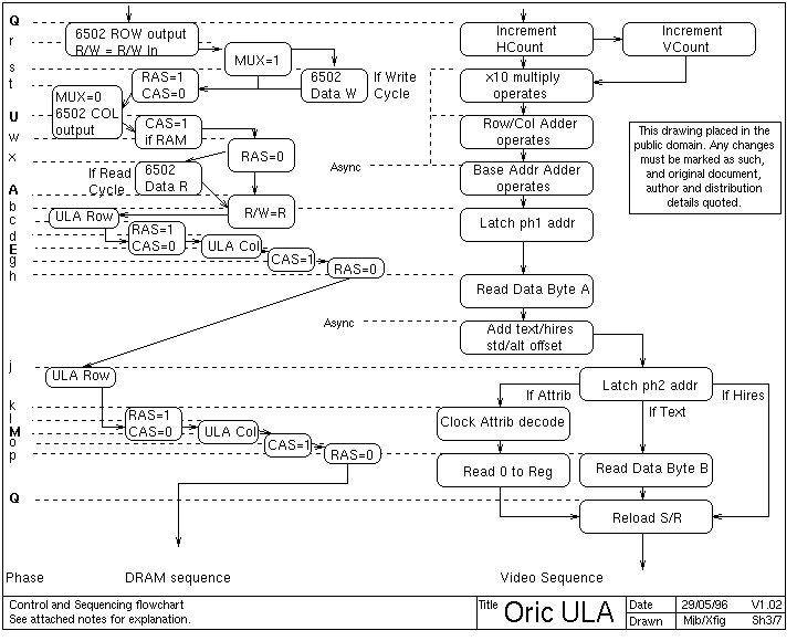
Having made many timing measurements, I can now state the contents and operation of this section with more confidence. The flowchart on sheet 3 shows a complete cycle (1 microsecond) of the ULA/processor combination. Each of the phases of operation are marked with a letter (Q through to Q), and should be viewed alongside the timing diagram of sheet 1.
At time "Q" the 1 MHz clock has just risen, and this clocks the horizontal counter, and possibly the vertical counter (by carry). This results in a new pair of values being available. These new values are multiplied by 10, added to each other, and added to the base address for the mode in force. No clocks are used to control this process, hence (ASYNChronous). By time "b", this will have stabilised, and the address is latched into the phase 1 address.
Meanwhile, at "Q", the 6502 phase began. So it will have a valid address on the main address bus. The R/W out follows ~R/W in, MUX is asserted to allow the row address through the external multiplexer. Then :-
For a Write cycle, the 6502 places its data at time "s". RAS is asserted. Then MUX is returned to 0, and the column address is presented through the ULA at "t". CAS is asserted, but only if this is actually a RAM write. Note that it is asserting CAS here that performs the write.
For a Read cycle, RAS is asserted. MUX iz returned to 0, and the column address is presented through the ULA at time "t". CAS is asserted, if this is a RAM access, and the data is read by the 6502 some time later at "x".
The DRAM R/W is then forced to "read". The ULA access cycle begins.
The Phase 1 address developed above is passed as first the ROW and then the COL address in two parts, asserting RAS and CAS respectively. At time "h", the available data is read and transferred to the holding register for the S/R. It is not yet known whether this will be used. It is also available at the input of the attribute decode, but it is not known whether it can be used.
Some time after the byte is read, the result of adding the text/hires offset and std/alt charset offset is available, and latched as phase 2 address at "j"
In this way we have covered all possibilities of dataflow for text/hires or attribute. Next, irrespective of mode, the phase 2 address is output as ROW/COL as before. If this is hires mode, the data so retrieved is ignored, the S/R is loaded from the previous value above, and the cycle ends. If text mode, the data byte retrieved is the bit image of the character set, and is loaded to the holding register over the (now known to be) ASCII value previously held. If this is an attribute, it is processed at "k", updating the selectors, and 0 (paper colour) is loaded to the holding register at "p"
At time Q the shift register reloads, and the cycle begins from the top.
These timings are partly speculative, and are derived from actual measurement of external signals as on sheet 1, and fitting internal operations in the correct order between these externally visible activities.
Also note that the ULA looks up and throws away much information. This results in a simpler design, and does no harm. So far, we have accesses that extend beyond the right and bottom edge of the screen, and also now character definition lookups in Hires mode, and even for attributes!
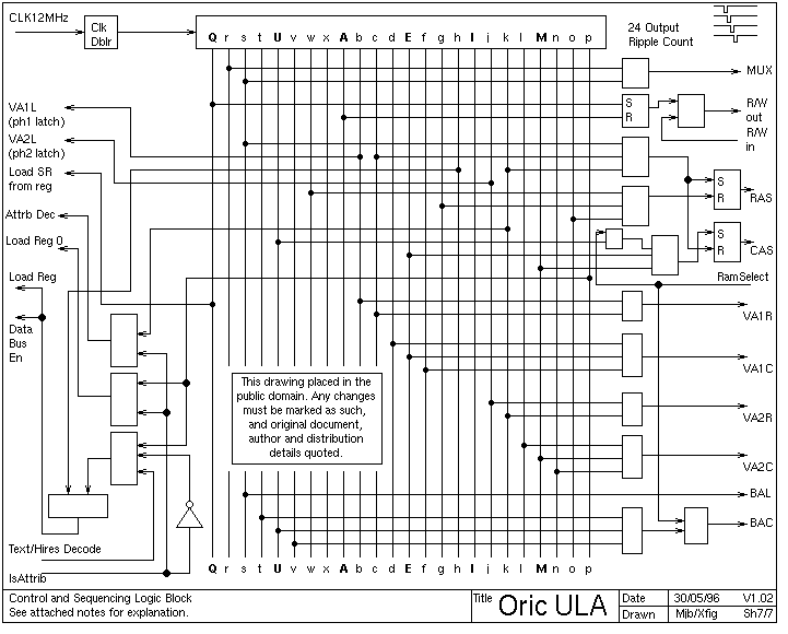
So from this, we can develop the sequencer logic as on sheet 7. Although this looks frightening, the behaviour echos that of the flowchart and timing diagram above.
The chip at the top provides a moving pulse, from "Q" through to "p". This moves along on *both* transitions of the 12 MHz clock, giving the 24 time slots used above.
Each signal can be derived by combinatorial logic from these. For example, working down the right side :-
MUX is active in time slots "r" and "s"
R/W follows R/W in from "Q" to "x", and is forced to read from "A" onwards.
RAS is asserted at times "s","c" and "k". Coincidentally, CAS is deasserted.
RAS is deasserted at times "w","g","o".
CAS is asserted at times "u","e","m". Note "U" is the 6502 access, and
depends on this actually *being* a RAM access!
VA1R is enabled through times "b" and "c"
...etc...
BAC is enabled to at times "t" though "v", but again only if the 6502 is
actually doing a RAM access.
Down the left, we have :-
...etc...
AttrbDec is active at "k" if the byte fetched is an attribute.
Load Reg 0 is active at "p" if the byte fetched is an attribute.
Data Bus is enabled at "h" to get the first byte (also into reg via "Load
Reg")
Data Bus is further enabled at "p" if *not* an attribute, and *not* hires
mode to get the character definition data (also into reg via "Load Reg")
Finally, this section replaces the old Figure 1 (speculative video timings) with actual measured figures. Shown at the top is one single line across the screen. The sync pulse occurs during counts 49,50,51 and 52 of the horizontal count. Note that the 1 MHz clock is shown only for reference against the timings - the count increments on rising edges of the 1 MHz clock.
The lower digram shows the last 4 scanlines, and then the vertical interval. The sync pulse here is 4 scanlines long (note that there are no "serrations", positive going horizontal pulses during the vertical sync).
>Although this schematic is in no way a complete circuit, it outlines the
>essential building blocks of the ULA. I am now working on filling out some of
>the detail, but would like some feedback on the project as it is to see if
>people agree with the design so far. I also need some time to make some
>actual timing measurements, and do a few programming tests. Maybe a handful
>of revisions down the line we'll have a 12 inch square piece of veroboard
>smothered with TTL, radiating heat and RFI like no tomorrow, piggybacked into
>an Oric, and *working*!
>
>The vision is there ....
The schematic now is probably one step away from a TTL based design. Unfortunately, some of the chips described here have no direct TTL counterpart - eg 24 output ripple count, 13 bit adder ... so these would have to be constructed from multiple chips.
However, I've been looking tentatively at some IC datasheets, and have found some very useful looking chips which are programmable logic arrays. These allow you to download a bit pattern specifying routing between logic blocks, and may be the way to go for re-building (and then, improving) the ULA. It would certainly be better for design modification than TTL. However, the programmer and software for these chips may not be cheap - I shall find out more .....
This document written by M.J. Brown, May-Jun 1996. It is placed in the public domain - however you must cite the title, author and contact points as given at the head of this document when quoting, modifying, or distributing this document and figures. This paragraph must remain intact. Any incomplete or modified distribution must be marked as such.